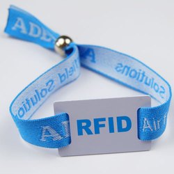
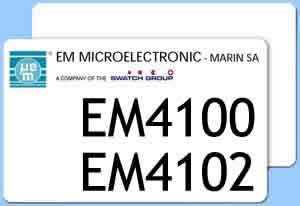
EM4100 WRISTBAND
EM4100 (previously named is a CMOS integrated circuit for use in electronic Read Only RF Transponders. The circuit is powered by an external coil placed in an electromagnetic field, and gets its master clock from the same field via one of the coil terminals. By turning on and off the modulation current, the chip will send back the 64 bits of information contained in a factor y pre-programmed memory array. The programming of the chip is performed by laser fusing of polysilicon links in order to store a unique code on each chip. The EM4100 has several metal options which are used to define the code type and data rate. Data rates 64, 32 and 16 periods of carrier frequency per data bit are available. Data can be coded as Manchester, Biphase or PSK. Due to low power consumption of the logic core, no supply buffer capacitor is required. Only an external coil is needed to obtain the chip function. A parallel resonance capacitor pF is also integrated. Features 64 bit memory array laser programmable Several options of data rate and coding available On chip resonance capacitor On chip supply buffer capacitor On chip voltage limiter Full wave rectifier on chip Large modulation depth due to a low impedance modulation device Operating frequency – 150 kHz Very small chip size convenient for implantation Very low power consumption Applications Logistics automation Anticounterfeiting Access control Industrial transponder Coil terminal / Clock input Coil terminal Parameter Maximum DC Current forced & COIL2 Power Supply Storage Temp. Die form Storage Temp. PCB form Electrostatic discharge maximum to MIL-STD-883C method 3015 Symbol ICOIL VDD Tstore VESD Conditions +125°C 1000V The AC Voltage on Coil is limited by the on chip voltage limitation circuitry. This is according to the parameter Icoil in the absolute maximum ratings. Parameter Operating Temp. Maximum Coil Current AC Voltage on Coil Supply Frequency Symbol Top ICOIL Vcoil fcoil Min. -40 Typ. Max. Units 10 mA Vpp kHz Stresses above these listed maximum ratings may cause permanent damage to the device. Exposure beyond specified operating conditions max affect device reliability or cause malfunction. This device has built-in protection against high static voltages or electric fields; however due to the unique properties of this device, anti-static precautions should be taken as for any other CMOS component. Electrical Characteristics VDD = 1.5V, VSS = 134kHz square wave, = 1.0V with positive peak at VDD and negative peak at VDD -1V unless otherwise specified Parameter Supply Voltage Rectified Supply Voltage – Coil2 Capacitance Power Supply Capacitor Biphase & Manchester Versions Supply Current C2 pad Modulator ON voltage drop C1 pad Modulator ON voltage drop PSK Version Supply Current PSK C2 pad Modulator ON voltage drop VDD VDDREC Cres Csup IDD VDD=5.0V IVDDC2=100µA with ref. to VDD IVDDC2=1mA with ref. to VDD IVDDC1=1mA with ref. to VDD = 2.8 VDC Modulator switch = “ON” Vcoil=100mVRMS f=10kHz The maximum voltage is defined by forcing – COIL2 The tolerance of the resonant capacitor ± 15% over the whole production. Optional reduced tolerance on request On a wafer basis, the tolerance ± 2% VDD = 1.5V, VSS = 0V, fcoil = 134kHz square wave, = 1.0V with positive peak at VDD and negative peak at VDD -1V unless otherwise specified Timings are derived from the field frequency and are specified as a number of RF periods. Parameter Read Bit Period Symbol Trdb Test Conditions depending on option Value 32, 16 Units RF periods


