AT88SC153,
Features
• One 64 x 8 (512-bit) Configuration Zone
• Three 64 x 8 (512-bit) User Zones
• Programmable Chip Select
• Low-voltage Operation: 2.7V to 5.5V
• Two-wire Serial Interface
• 8-byte Page Write Mode
• Self-timed Write Cycle (10 ms max)
• Answer-to-reset Register
• High-security Memory Including Anti-wiretapping
– 64-bit Authentication Protocol (under exclusive patent license from ELVA)
– Secure Checksum
– Configurable Authentication Attempts Counter
– Two Sets of Two 24-bit Passwords
– Specific Passwords for Read and Write
– Four Password Attempts Counters
– Selectable Access Rights by Zone
• ISO Compliant Packaging
• High Reliability
– Endurance: 100,000 Cycles
– Data Retention: 100 Years
– ESD Protection: 4,000V min
• Low-power CMOS
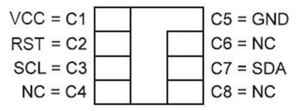
Table 0-1. Pin Configuration
| Name | Description | ISO Module Contact | Standard Package Pin |
| VCC | Supply Voltage | C1 | 8 |
| GND | Ground | C5 | 1 |
| SCL | Serial Clock Input | C3 | 6 |
| SDA | Serial Data Input/Output |
C7 | 3 |
| RST | Reset Input | C2 | 7 |
8-pin SOIC or, PDIP
The AT88SC153 provides 2,048 bits of serial EEPROM memory organized as one configuration zone of 64 bytes and three user zones of 64 bytes each. This device is optimized as a “secure memory” for multiapplication smart card markets, secure identification for electronic data transfer, or components in a system without the requirement of an internal microprocessor. The embedded authentication protocol allows the memory and the host to authenticate each other. When this device is used with a host that incorporates a microcontroller (e.g., AT89C51, AT89C2051, AT90S1200), the system provides an “anti-wiretapping” configuration. The device and the host exchange “challenges” issued from a random generator and verify their values through a specific cryptographic function included in each part. When both agree on the same result, the access to the memory is permitted.
Depending on the device configuration, the host might carry out the authentication protocol and/or present different passwords for each operation, read or write. Each user zone may be configured for free access for read and write or for password-restricted access. To insure security between the different user zones (multiapplication card), each zone can use a different set of passwords. A specific attempts counter for each password and for the authentication provides protection against “systematic attacks.” When the memory is unlocked, the two-wire serial protocol is effective, using SDA and SCL. The memory includes a specific register providing a 32-bit data stream conforming to the ISO 7816-10 synchronous answer-to-reset.
Pin Descriptions
The VCC input is a 2.7V-to-5.5V positive voltage supplied by the host.
The SCL input is used to positive edge clock data into the device and negative edge clock data out of the device.
The SDA pin is bidirectional for serial data transfer. This pin is open-drain driven and may be wire-ORed with any number of other open-drain or open-collector devices. An external pull-up resistor should be connected between SDA and VCC. The value of this resistor and the system capacitance loading the SDA bus will determine the rise time of SDA. This rise time will determine the maximum frequency during read operations. Low value pull-up resistors will allow higher frequency operations while drawing higher average power supply current.
When the RST input is pulsed high, the device will output the data programmed into the 32-bit answer-to-reset register. All password and authentication access will be reset. Following a reset, device authentication and password verification sequences must be presented to re-establish user access.
The 2,048 bits of the memory are divided in four zones of 64 bytes each.
FAB, CMA, and PER are nonvolatile fuses blown at the end of each card life step. Once blown, these EEPROM fuses can not be reset.
• The FAB fuse is blown by Atmel prior to shipping wafers to the card manufacturer.
• The CMA fuse is blown by the card manufacturer prior to shipping cards to the issuer.
• The PER fuse is blown by the issuer prior to shipping cards to the end user.
The device responds to a read fuse command with fuse byte.
| Bit 7 | Bit 6 | Bit 5 | Bit 4 | Bit 3 | Bit 2 | Bit 1 | Bit 0 |
| 0 | 0 | 0 | 0 | 0 | PER | CMA | FAB |
When the fuses are all “1”s, read and write are allowed in the entire memory. Before blowing the FAB fuse, Atmel writes the entire memory to “1” and programs the fabrication subzone (except CMC and AR) and the secure code.
| Access Rights | ||||
| Zone | Access | FAB = 0 | CMA = 0 | PER = 0 |
| Fabrication (Except CMC, MTZ and AR) |
Read | Free | Free | Free |
| Write | Forbidden | Forbidden | Forbidden | |
| Card Manufacturer Code |
Read | Free | Free | Free |
| Write | Secure Code | Secure Code | Secure Code | |
| Access Registers | Read | Free | Free | Free |
| Write | Secure Code | Secure Code | Secure Code | |
| Memory Test Zone | Read | Free | Free | Free |
| Write | Free | Free | Free | |
| Identification | Read | Free | Free | Free |
| Write | Secure Code | Secure Code | Forbidden | |
| Secret | Read | Secure Code | Secure Code | Forbidden |
| Write | Secure Code | Secure Code | Forbidden | |
| Passwords | Read | Secure Code | Secure Code | Write PW |
| Write | Secure Code | Secure Code | Write PW | |
| PAC | Read | Free | Free | Free |
| Write | Secure Code | Secure Code | Write PW | |
| User Zones | Read | AR | AR | AR |
| Write | AR | AR | AR | |
Note: CMC: Card Manufacturer Code
AR: Access Rights as defined by the access registers
PW: Password
Answer-to-reset: 32-bit register defined by Atmel
Lot History Code:32-bit register defined by Atmel
Fab Code:16-bit register defined by Atmel
Card Manufacturer Code:16-bit register defined by the card manufacturer
Issuer Code:64-bit register defined by the card issuer
Access Registers:Three 8-bit access registers defined by the issuer, one for each user zone (active low)
| Bit 7 | Bit 6 | Bit 5 | Bit 4 | Bit 3 | Bit 2 | Bit 1 | Bit 0 |
| WPE | RPE | ATE | AOW | PWS | WLM | MDF | PG |
Write Password Enable (WPE): If enabled (WPE = “0”), the user is required to verify the write password to allow write operations in the user zone. If disabled (WPE = “1”), all write operations are allowed within the zone. Verification of the write password also allows the read and write passwords to be changed.
Read Password Enable (RPE): If enabled (RPE = “0”), the user is required to verify either the
read password or write password to allow read operations in the user zone. Read operations initiated without a verified password will return $00 (or the status of the fuse bits, if either CMA or
PER are still intact). Verification of the write password will always allow read access to the zone.
RPE = “0” and WPE = “1” is allowed but is not recommended.
Authentication Enable (ATE): If enabled (ATE = “0”), a valid authentication sequence is required for both read and write and must be completed before access is allowed to the user zone. If disabled (ATE = “1”), authentication is not required for access.
Authentication Only for Write (AOW): If enabled (AOW = “0”), a valid authentication sequence
must be completed before write access is allowed to the user zone. Read access to this zone is
allowed without authentication. This bit is ignored if ATE is enabled.
Password Select (PWS): This bit defines which of the two password sets must be presented to
allow access to the user zone. Each access register may point to a unique password set, or access registers for multiple zones may point to the same password set. In this case, verification of a single password will open several zones, combining the zones into a single larger zone.
Write Lock Mode (WLM): If enabled (WLM = “0”), the 8 bits of the first byte of each user zone
page will define the locked/unlocked status for each byte in the page. Write access is forbidden
to a byte if its associated bit in byte 0 is set to “0”. Bit 7 controls byte 7, bit 6 controls byte 6, etc.
Modify Forbidden (MDF): If enabled (MDF = “0”), no write access is allowed in the zone at any
time. The user zone must be written before the PER is blown.
Program Only (PGO): If enabled (PGO = “0”), data within the zone may be changed from “1” to
“0” but never from “0” to “1”.
Identification Number (Nc):An identification number with up to 56 bits is defined by the issuer and should be unique for each device.
Cryptogram (Ci):The 56-bit cryptogram is generated by the internal random generator and modified after each successful verification of the cryptogram by the chip, on host request. The initial value, defined by the issuer, is diversified as a function of the identification number. The 64 bits used in the authentication potocol consist of the 56-bit cryptogram and the 8-bit uthentication Attempts Counter (AAC). Note that any change in the AAC status will change Ci for the next authentication attempt.
Secret Seed (Gc):The 64-bit secret seed, defined by the issuer, is diversified as a function of the identification number.
Memory Test Zone:The memory test zone is an 8-bit free access zone for memory and protocol test.
Password Set:The password set consists of two sets of two 24-bit passwords for read and write operations, defined by the issuer. The write password allows modification of the read and write passwords of the same set. By default, Password 1 is selected for all user zones.
Secure Code: The secure code is a 24-bit password defined by Atmel and is different for each card manufacturer. The Write 1 Password is used as the secure code until the personalization is over (PER = 0).
Attempts Counters: There are four 8-bit password attempts counters (PACs), one for each password, and one other 8-bit attempts counter for the authentication protocol (AAC). The attempts counters limit the number of consecutive incorrect code presentations allowed (currently
four).
Device Configuration Register:This 8-bit register allows the issuer to select the device configuration options (active-low).
| Bit 7 | Bit 6 | Bit 5 | Bit 4 | Bit 3 | Bit 2 | Bit 1 | Bit 0 |
| SME | UCR | UAT | ETA | CS3 | CS2 | CS1 | CS0 |
Programmable Chip Select (CS0–CS3): The four most significant bits (b4–b7) of every command comprise the chip select address. All AT88SC153 devices will respond to the default chip select address of $B (1011). Each device will also respond to a second chip select address programmed into CS0–CS3 of the device configuration register. By programming each device to a unique chip select address, it is possible to connect up to 15 devices on the same serial data bus. The Write EEPROM and Verify Password commands can be used globally to all devices sharing the bus by using the default chip select address $B.
Eight Trials Allowed (ETA): If enabled (ETA = “0”), the ETA extends the trials limit to eight incorrect presentations allowed (passwords or authentication). If disabled (ETA = “1”), the PAC and AAC will allow only four incorrect attempts.
Unlimited Authentication Trials (UAT): If enabled (UAT = “0”), the AAC is disabled, allowing an unlimited number of authentication attempts. The PACs are not affected by the UAT bit.
Unlimited Checksum Reads (UCR): If enabled (UCR = “0”), the device will allow an unlimited number of checksums without requiring a new authentication.
Supervisor Mode Enable (SME): If enabled (SME = “0”), verification of the Write 1 password will allow the user to write and read the entire passwords zone (including the PACs).
After a valid authentication has been completed, the internal pseudo-random generator (PRG) will compute a secure checksum after one write command or several consecutive write commands. This checksum certifies that the data sent by the host during the write commands were received and therefore written in the memory. For every write command, the device clocks the data bytes into the PRG and its output is the Checksum Authentication Register (CAR), which is a function of Ci, Gc, Q, and the data bytes written.
After a valid authentication, any write command will enable the checksum mode and cause AAC to become the virtual location of the 8-byte CAR. When all data have been transmitted, the host may perform a Read CAR command by sending a read command with the AAC address ($20). The first 8 bytes transmitted by the device form the secure checksum.
The checksum mode allows only a single Read CAR operation for each valid authentication. The checksum mode is disabled at the end of the Read CAR command, whatever the number of bytes transmitted, or by a read command with any other address. The checksum mode can only be enabled once for a given authentication.
Note: During the Read CAR command, the internal address counter is incremented just as in a normal read command. Once 8 bytes have been transmitted, the checksum mode is automatically disabled, and if the host continues to request data, the device responds as to a normal read command, from the address $28.
Ordering Information
| Ordering Code | Package | Voltage Range | Temperature Range |
| AT88SC153-09ET-00 | M2 – E Module | 2.7V–5.5V | Commerical (0°C–70°C) |
| AT88SC153-09PT-00 | M2 – P Module | 2.7V–5.5V | Commerical (0°C–70°C) |
| AT88SC153-10PU-00 | 8P3 | 2.7V–5.5V | Industrial (− 40°C–85°C) |
| AT88SC153-10SU-00 | 8S1 | 2.7V–5.5V | Industrial (− 40°C–85°C) |
| AT88SC153-10WU-00 | 7 mil Wafer | 2.7V–5.5V | Industrial (− 40°C–85°C) |
| Package Type | Description |
| M2 – P Module | M2 ISO 7816 Smart Card Module with Atmel Logo |
| M2 – E Module | M2 ISO 7816 Smart Card Module |
| 8S1 | 8-lead, 0.150” Wide, Plastic Gull Wing Small Outline Package (JEDEC SOIC) |
| 8P3 | 8-lead, 0.300” Wide, Plastic Dual Inline Package (PDIP) |
| Notes: 1. Formal drawings may be obtained from an Atmel Sales Office. | |
Smart Card Modules
Module Size: M2-00
Glob Top: Clear, Round: Æ 8.0 [mm] max
Dimension*: 12.6 x 11.4 [mm]
Thickness: 0.58 [mm] max
Pitch: 14.25 [mm]
Module Size: M2
Dimension*: 12.6 x 11.4 [mm]
Glob Top: Square: 8.8 x 8.8 [mm]
Thickness: 0.58 [mm]
Pitch: 14.25 [mm]
*Note: The module dimensions listed refer to the dimensions of the exposed metal contact area. The actual dimensions of the module after excise or punching from the carrier tape are generally 0.4 mm greater in both directions (i.e., a punched M2 module will yield 13.0 x 11.8 mm).


Reviews
There are no reviews yet.